Skip main navigation

New offer! Get 30% off one whole year of Unlimited learning. Subscribe for just £249.99 £174.99. New subscribers only. T&Cs apply

Find out more

How does an electron microscope work?

Read more about how electron microscopes work and discover the different types of microscopes that are used for examining the nanoscale.
How An Electron Microscope Works
© University of York

What is an electron microscope?

An electron microscope uses a beam of electrons instead of light to create magnified images of very small objects. Described as waves, fast electrons can have wavelengths that are several orders of magnitude shorter than the wavelength of visible light.

For example:

[lambda = frac{h}{m_ev}]

where (lambda) is the electron wavelength, (h) is plank’s constant (6.63 x 10⁻³⁴ m2kg/s), (m_e) is the mass of the electron, and (v) is the velocity of the electron.

Accelerate the electrons

We can see that the higher the velocity of the electron, the shorter the wavelength, and the better the resolution of the microscope will be. Therefore the first thing we need to do is accelerate the electrons. We do this using a high voltage to create an electric field.

The kinetic energy ((E=frac{1}{2}m_ev^2)) that an electron gains when it is accelerated by an electric field is given by:

[E = VQ]

where (V) is the potential difference and (Q) is the charge on an electron ((e)).

Combining these equations tells us that the wavelength of an electron is given by:

[lambda = frac{h}{sqrt{2m_eeV}} = frac{1.23times10^{-9}}{sqrt{V}}]

So, for example, for an accelerating voltage of 60 kV the wavelength of the electrons is ~5 pm (5 ×10-12 m, or 0.005 nm).

This means that electron microscopes have to resolve power hundreds or thousands of times better than optical microscopes, which are limited to wavelengths of around 4×10⁻⁷m.

Magnetic fields

Because electrons are charged, they can be guided by magnetic fields. Therefore electron microscopes use electromagnetic lenses (coils) to guide and focus electrons – much like the glass lenses used in light microscopes. We can deflect and steer the electrons, just like the lenses in glasses bend and focus light.

This is very similar to the use of guiding magnetic fields in tokamaks, which we met last week when we looked at fusion energy. We use these magnetic fields to ensure the electron beam hits the sample in the correct place, and has the right size.

As we will see below, exactly what place and size we choose depends on what type of microscope we are building.

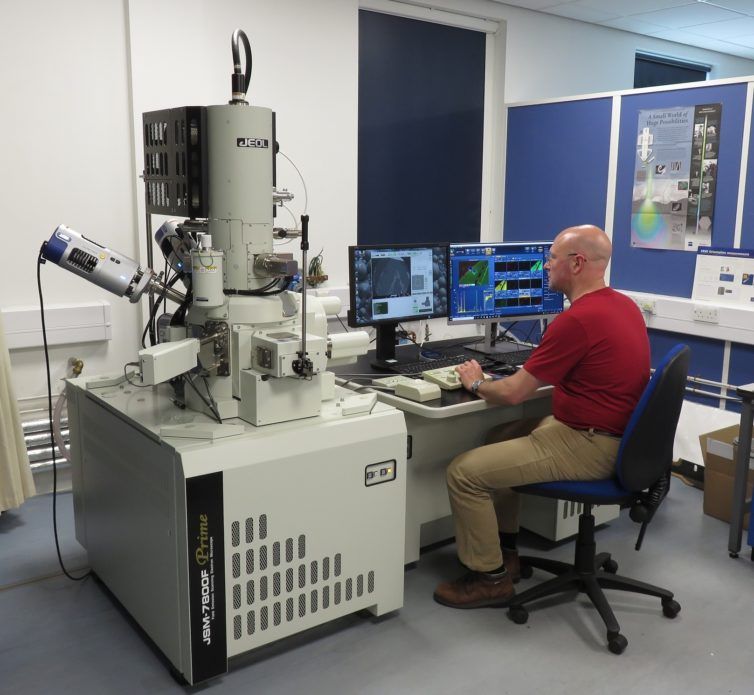
Electron microscopes come in different sizes, geometries and abilities.

Scanning Electron Microscopes (SEM)

Scanning Electron Microscopes (SEM) are the smaller type of electron microscope and operate a so-called reflection geometry. The images of the specimens are created by scanning across the surfaces of specimens with a focused beam of electrons (typically accelerated by voltages of between 5-30 kV).

Most of the beam electrons are reflected or scattered backwards (hence the term reflection geometry), having interacted with atoms close to the surface of the sample.

These electrons are collected by detectors and their intensity contains information about the sample’s surface characteristics. Typical SEM magnifications are about x100,000 times, with resolutions reaching about 10nm.

Transmission Electron Microscopes (TEM)

Transmission Electron Microscopes (TEM) use a broad electron beam to illuminate very thin, electron-transparent specimens, typically below 100 nm in thickness.

To be able to pass through the samples, the electrons are typically accelerated to higher energies compared to those used in an SEM (using accelerating voltages of 60 – 300 kV). The transmitted electrons carry information about the structure of the specimen.

The magnified image is formed by the objective lens system and is viewed by being projected onto a fluorescent viewing screen or a digital camera. Modern high-resolution TEM microscopes can reach magnifications well above 1,500,000 times.

Scanning Transmission Electron Microscopes (STEM)

Scanning Transmission Electron Microscopes (STEM) are a crossover between SEM and TEM microscopes. Similar to TEM, STEM uses transmission and very thin electron-transparent specimens are needed. However, like SEM, a small electron beam is not static but is scanned along with the sample.

In STEM, the transmitted electrons are collected by detectors and the image is viewed with the help of a computer monitor. In modern high-resolution STEM microscopes, the electron probe can be focused down to sizes well below that of an individual atom (typical atom diameter ~0.1 nm or 10-10 m), reaching magnifications of about x10,000,000 times.

An example of the kind of image you can attain with a STEM is shown below. It is a nanoparticle – a small nanometre-sized cluster of atoms.


© University of York
This article is from the free online

Frontier Physics, Future Technologies

Created by
FutureLearn - Learning For Life

Reach your personal and professional goals

Unlock access to hundreds of expert online courses and degrees from top universities and educators to gain accredited qualifications and professional CV-building certificates.

Join over 18 million learners to launch, switch or build upon your career, all at your own pace, across a wide range of topic areas.

Start Learning now